



Product Description
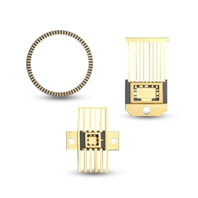
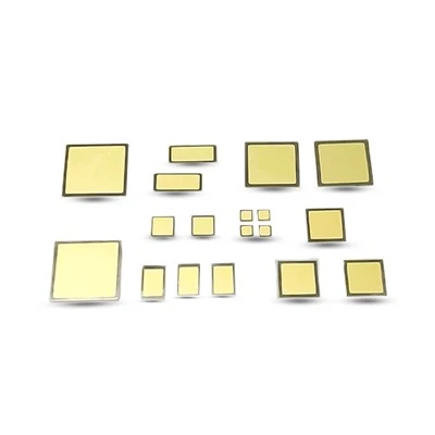
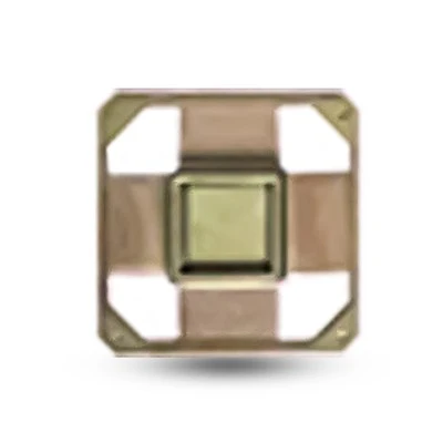
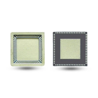
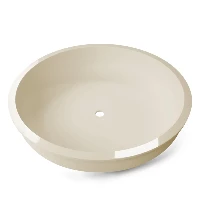
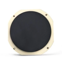
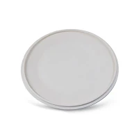
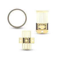
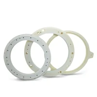
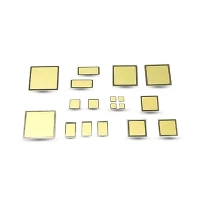
The core advantage of the SMD shells we supply is reflected in the efficiency of heat conduction and current carrying capacity. By optimizing the material scheme of the heat dissipation base, the product helps alleviate the temperature rise pressure of power components under high load. The metallized layer of the shell has stable quality, good conductivity and low resistivity characteristics, and has excellent resistance to environmental aging. We have a rich selection of standard specifications available for selection, and can also carry out professional technical matching for special application scenarios, providing material solutions with high adaptability, helping to stabilize the packaging production line.
Features
- Excellent heat dissipation performance
- Strong resistance to environmental aging and long service life
- Good electromagnetic compatibility (EMC)
- Supports high current-carrying capacity
- Strong long-term service stability
- Excellent electrical performance
- Good corrosion resistance
- High impact resistance
- Low coefficient of thermal expansion (CTE)
- High moisture resistance
Main Model Table (mm)
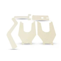
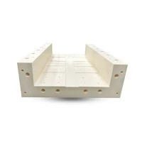
SMD packages feature Alumina or AlN substrates with heat sink options in CuW, MoCu, or OFC. We offer full-scale customization with precise material cross-referencing and technical conversion from drawings or physical samples to accurately match diverse and specialized component requirements.
Ceramic Expertise
Tessvida is a Total Kit Solutions (TKS) specialist, serving key industries: semiconductor & electronics, medical devices, FPD/LED, machinery, petrochemicals, auto & Transportation, energy & power, and food & agriculture. With a mature supply chain and advanced processes (isostatic pressing, gel casting, dry pressing), we offer end-to-end capabilities from material preparation, molding, sintering to precision machining and post-processing.
Backed by deep expertise in high-purity ceramics and strong resource integration, our flexible custom services precisely meet customer needs from material selection to finished product delivery.
Ceramic Production Process

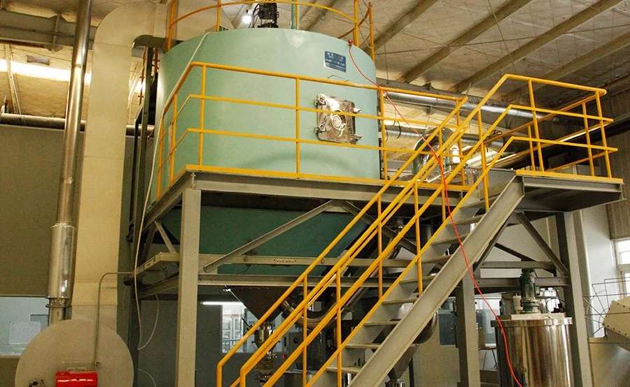
Powder Preparation
Raw material powder preparation, spray granulation (mixing, mechanical ball milling, spray drying)
01

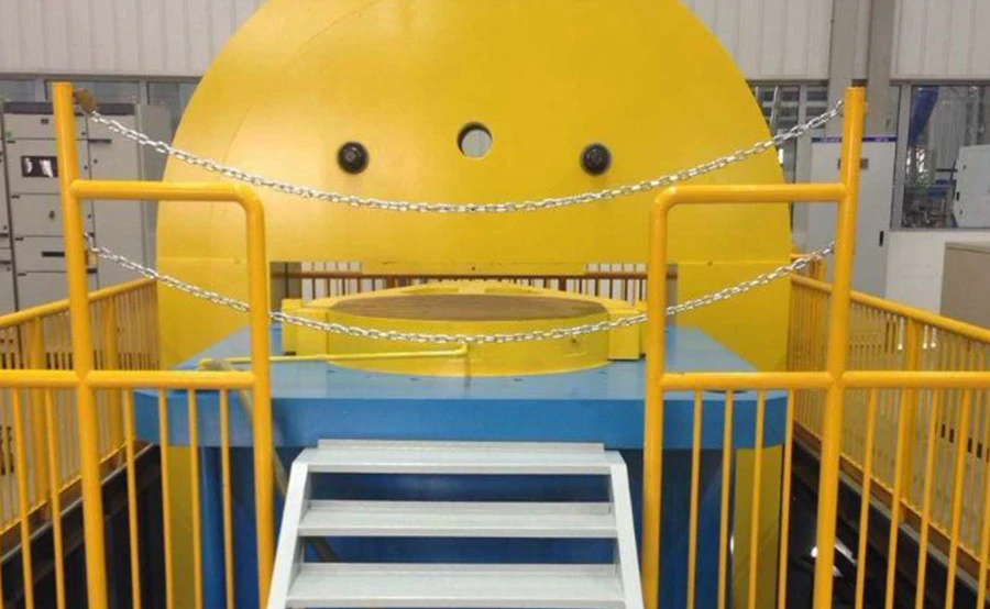
Powder Forming
Isostatic pressing, dry pressing, injection molding, gel forming, casting, hot pressing
02

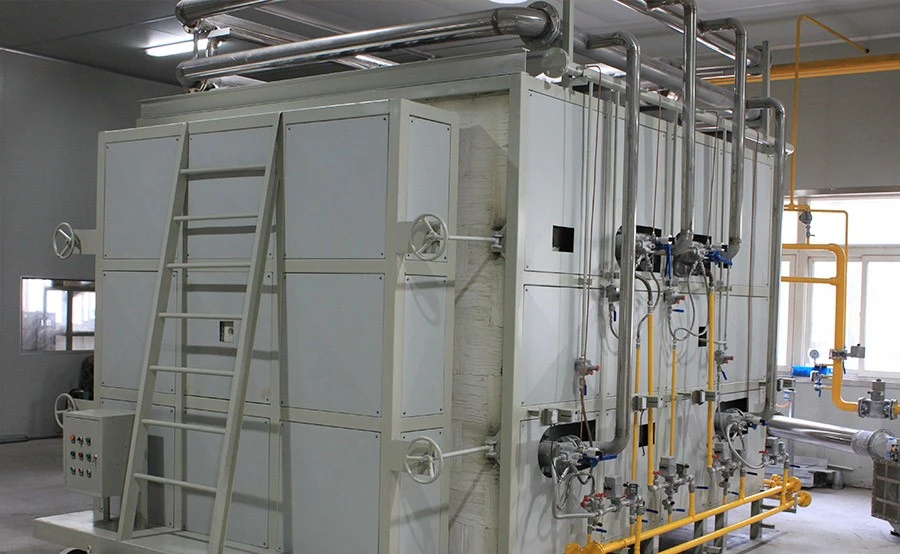
High-Temperature Sintering
Atmospheric sintering, vacuum sintering, controlled atmosphere sintering
03

Precision Processing
Cutting, turning, grinding, milling, shaping, drilling
04

Surface Treatment
Cleaning, arc melting, plasma spraying, electrostatic spraying, vapor deposition, ultra-clean cleaning, anodizing, metallization composite
05
Precision Ceramic Processing Workflow
-
Material Preparation
-
Material Forming
-
Sintering
-
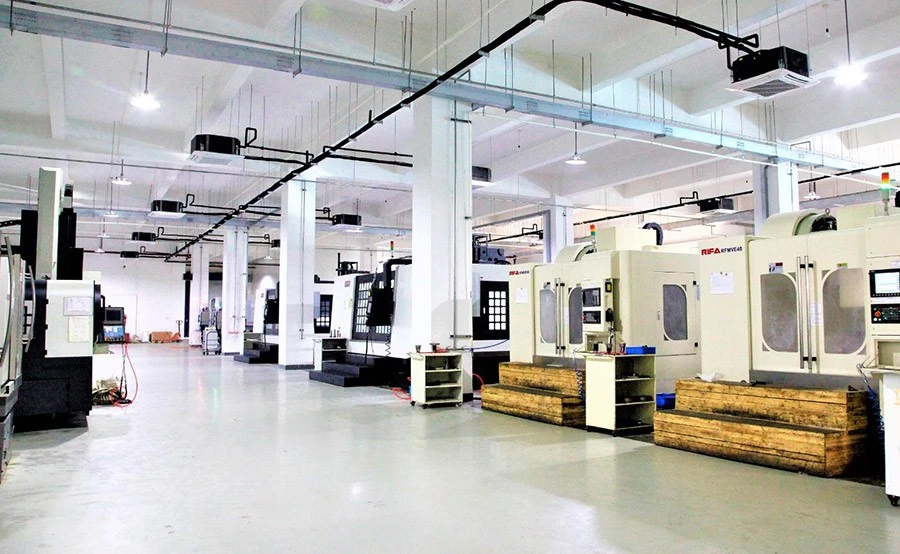
Fine Machining
-
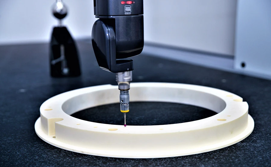
Inspection
-
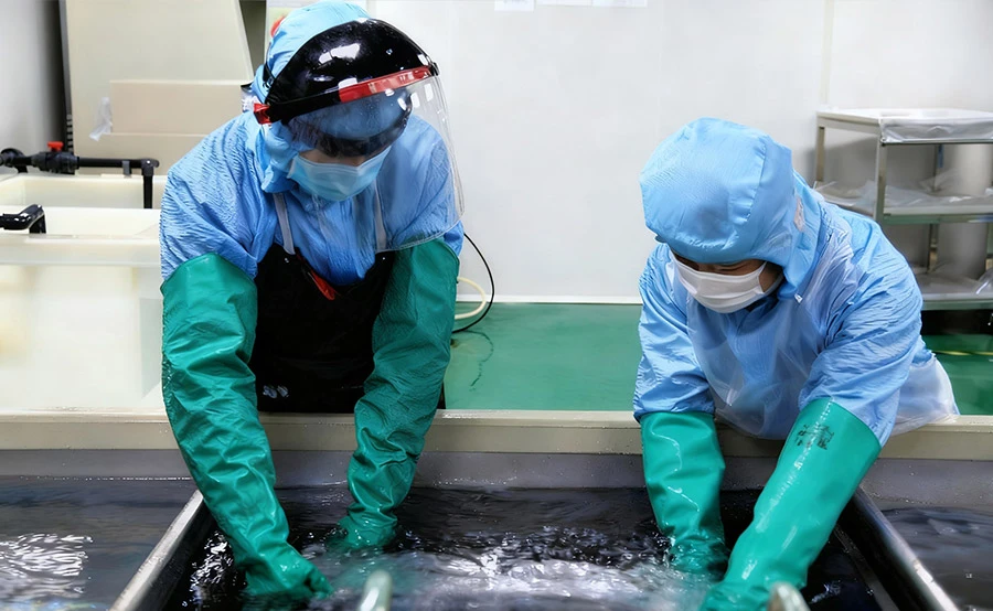
Precision Cleaning
-
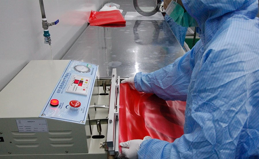
Vacuum Packing
-
Material Preparation
-
Material Forming
-
Sintering
-
Fine Machining
-
Inspection
-
Precision Cleaning
-
Vacuum Packing
Hot Tags: ceramic packages and smd package, ceramic packages and smd package manufacturers, suppliers, factory